TSMC Is Building an "EMIB-Like" Package — Why Advanced Packaging Is the New Battleground for AI Chips
One-line takeaway: As transistor scaling slows, stitching multiple chips together with high-speed bridges has become the key to AI performance — and TSMC's "EMIB-like" packaging push with substrate maker Kinsus is a direct challenge to Intel's proprietary packaging moat.
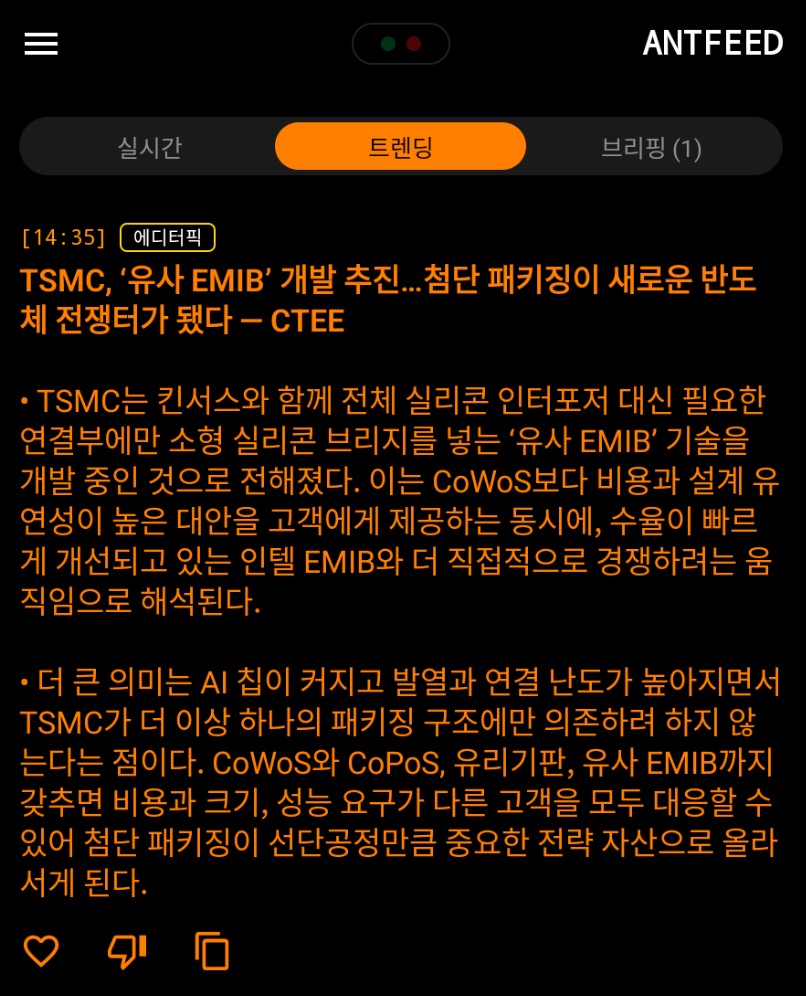
The hottest topic in semiconductors right now isn't which chip got smaller — it's a far more physical question: if chips can't keep shrinking, how do they keep getting faster? The answer is advanced packaging. And this time, TSMC is taking aim at Intel's signature EMIB technology.
What is "EMIB-like" packaging, and why is TSMC chasing Intel's tech?
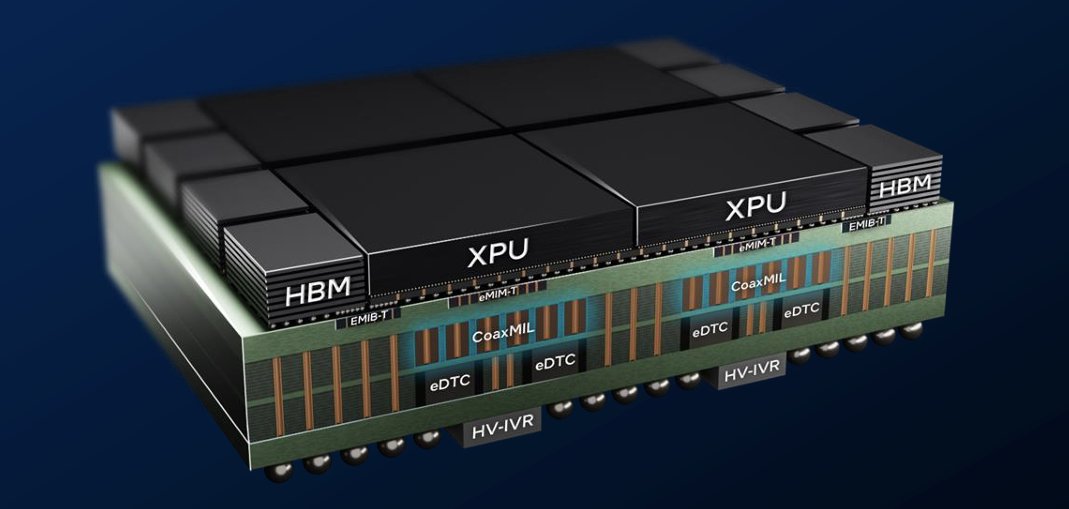
EMIB (Embedded Multi-die Interconnect Bridge) is Intel's flagship packaging approach. The idea: embed a tiny silicon bridge into the substrate, connecting only the chip regions that need high-speed communication — no need to replace the entire substrate with an expensive silicon interposer.
For years, EMIB has been the counterweight to TSMC's dominant CoWoS. Now TSMC is reportedly developing an "EMIB-like" packaging technology with Kinsus, a major ABF substrate maker, to support larger multi-die AI chips and reduce reliance on capacity-constrained CoWoS — stepping directly into Intel's moat.
CoWoS, InFO, EMIB: three advanced packaging approaches, explained
- CoWoS (TSMC): Logic chips and HBM memory sit side-by-side on a silicon interposer. The interposer is large and expensive, but virtually every AI accelerator depends on it — capacity has been "maxed out" for a long time.
- InFO (TSMC): Skips the silicon interposer for a cheaper fan-out substrate. Lower cost, used for applications that don't need HBM.
- EMIB (Intel): No full interposer — small silicon bridges are embedded only where needed. Flexible and relatively cost-controlled, but the yield and supply-chain ecosystem are Intel-led.
In plain terms: CoWoS is like tiling the whole floor with marble; EMIB is like laying premium tiles only on the corridors — cheaper, but technically harder. TSMC's "EMIB-like" version aims to deliver EMIB's flexibility using its own substrate and supply-chain muscle, without paying Intel's patent toll.
Why this move ripples through the global AI supply chain
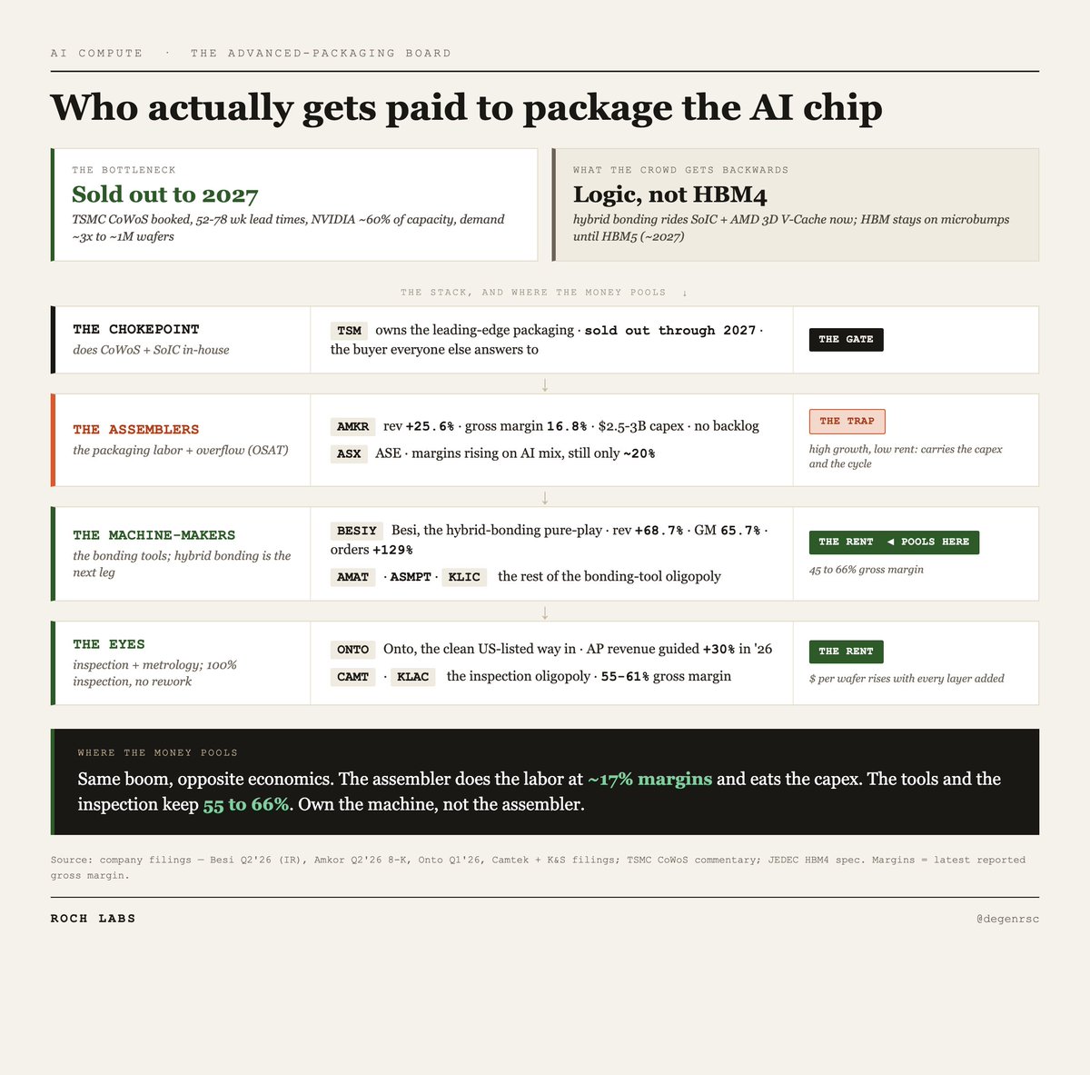
The market reacted immediately: TSMC's ADR jumped more than 7% on the news, and analysts flagged multiple packaging and substrate suppliers as beneficiaries. Three layers of logic explain it:
1. Capacity bottleneck: AI chip demand has CoWoS running at full capacity, with customers queuing for months. A second "EMIB-like" technology route is another shipping lane.
2. Patents and ecosystem: Intel's EMIB ecosystem has attracted interest from Nvidia, and Google reportedly ordered over 3 million custom AI processors from Intel for 2028. If TSMC can offer an equivalent with its own technology, customers stay inside its ecosystem.
3. Supply-chain spread: Advanced packaging is no longer just a foundry game — substrate, packaging, and materials players have all become strategic links. ABF substrates are now described as "strategic materials."
Investor perspective: real beneficiary vs. trend-chasing hype
When a technology trend heats up, markets always produce a wave of "theme stocks." Three questions help separate fact from fiction: Is this company actually in the advanced-packaging supply chain? Are orders confirmed or merely "possible"? Does the technology barrier create a real moat? For substrate and packaging firms, profits ultimately depend on yield ramp and customer qualification — not on headlines.
The advanced packaging arms race has only just begun. TSMC challenging Intel, Chinese players pushing glass substrates — the global supply-chain map is being redrawn. Whoever can ramp volume production and lock in big customers wins the next round of the AI chip war.
FAQ
Q1: What's the real difference between CoWoS and EMIB?CoWoS uses a full silicon interposer to connect chips and HBM — large and expensive. EMIB embeds small silicon bridges only where high-speed links are needed — cheaper but technically complex. Both are multi-die approaches that break the single-chip area limit.
Q2: Why does advanced packaging matter more as Moore's Law slows?Transistor scaling gets exponentially more expensive. Manufacturers instead package multiple mature-process chips together to boost overall performance — advanced packaging is the new path to performance growth.
Q3: Who is Kinsus, and why did ABF substrates suddenly become strategic?Kinsus is a major ABF substrate maker. Advanced packaging and high-end chips both need ABF substrates as their "foundation" — layer count and precision directly determine packaging yield, turning substrates into a critical AI supply-chain link.
Q4: Will "EMIB-like" packaging replace CoWoS?Not in the short or medium term — CoWoS remains the mainstream for AI accelerators, with demand far exceeding supply. The EMIB-like route is a second path for capacity and cost flexibility, giving TSMC a fuller menu for different customer needs.
Q5: How should investors approach this trend?Look for orders actually landing in financials, then judge technology barriers. Advanced packaging is a long-term structural trend, but yield ramps take time — short-term rallies often run ahead of fundamentals, so check valuations before chasing.
留言
張貼留言