跳到主要內容

台積電也來做「類 EMIB」封裝?當摩爾定律放緩,先進封裝為何成了 AI 晶片的新決戰點?

一句話結論: 當晶片微縮愈來愈慢,「把多顆晶片用高速橋接拼在一起」的先進封裝成了 AI 算力倍增的關鍵——台積電聯手景碩開發「類 EMIB」技術,正是要向英特爾獨門的封裝專利壁壘發起正面挑戰。
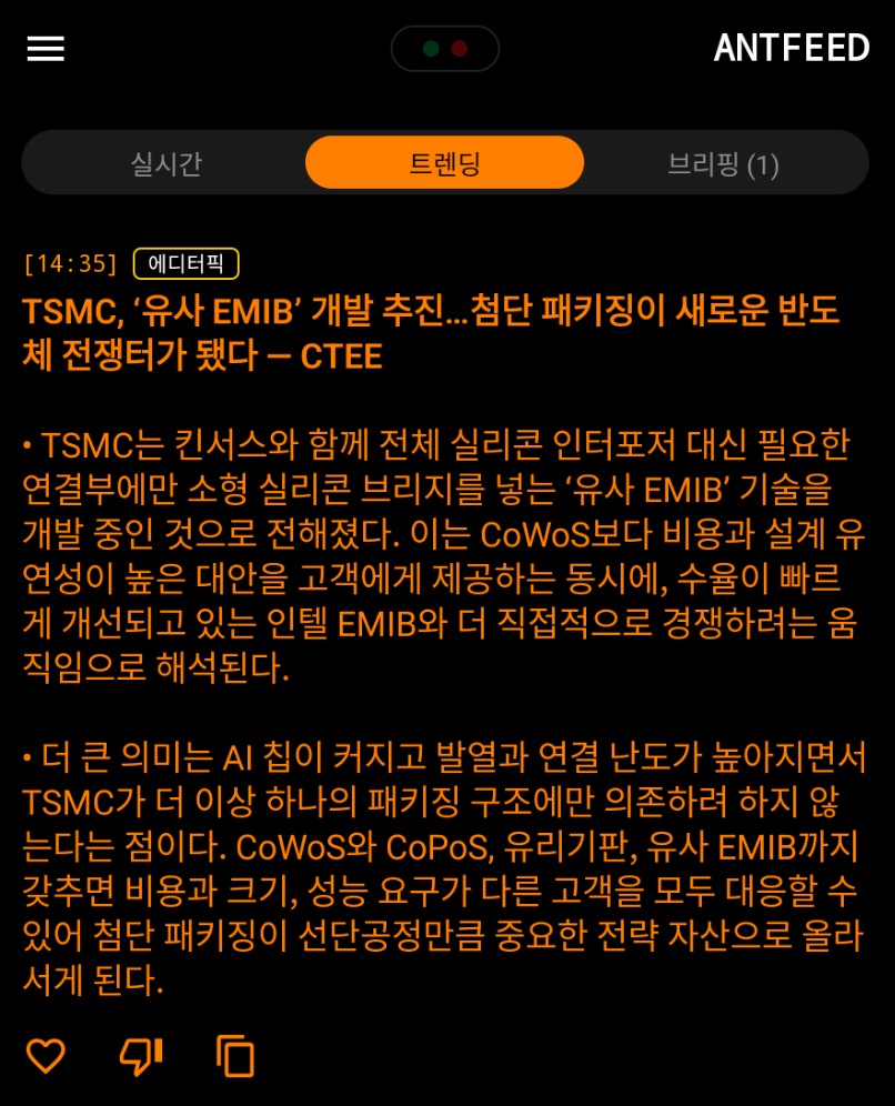
台積電進軍英特爾 EMIB 地盤——「矽橋」之爭正式開打

最近半導體圈最熱的話題不是哪一顆晶片又變小了,而是一個更「物理」的問題:晶片越做越小已經快到極限,接下來要靠什麼繼續變快? 答案指向先進封裝——而這一次,台積電把矛頭對準了英特爾的獨門技術 EMIB。

什麼是「類 EMIB」?為什麼台積電要追英特爾的技術?

EMIB(Embedded Multi-die Interconnect Bridge,嵌入式多晶片互連橋)是英特爾的招牌封裝技術。概念是:把一片極小的矽橋嵌入載板中,只讓需要高速溝通的晶片區塊透過這座橋互連,不需要把整塊載板都換成昂貴的矽中介層。

過去幾年,EMIB 一直與台積電主導的 CoWoS 分庭抗禮。如今傳出台積電與 ABF 載板大廠景碩合作、開發「類 EMIB」封裝技術,用於支援更大的多晶片 AI 晶片,並降低對產能吃緊的 CoWoS 的依賴——等於直接踏進英特爾的護城河。
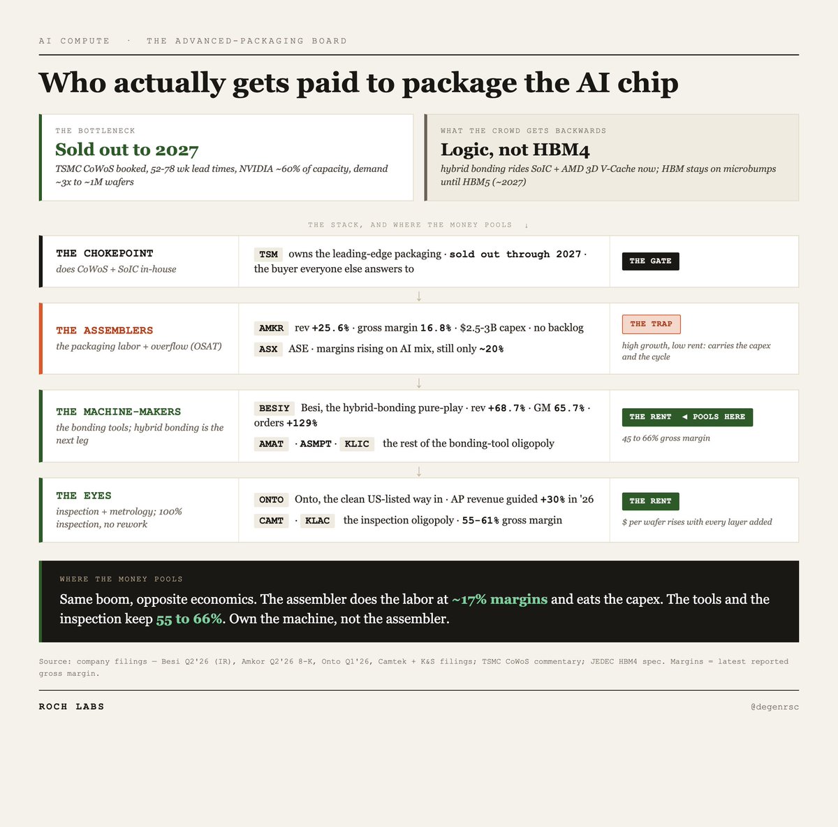
AI 晶片出貨的隱形瓶頸——先進封裝才是真正卡關的環節

CoWoS、InFO、EMIB:三種先進封裝一次看懂

  • CoWoS(台積電):把邏輯晶片與高頻寬記憶體(HBM)並排放置在矽中介層(silicon interposer)上。中介層面積大、成本高,但目前 AI 加速器幾乎都靠它,產能長期「吃到撐」。
  • InFO(台積電):捨棄矽中介層,改用更便宜的扇出型載板,成本較低,常用於不需要 HBM 的應用。
  • EMIB(英特爾):不鋪整片中介層,只在需要的地方嵌入小型矽橋。靈活、成本相對可控,但良率與供應鏈生態由英特爾主導。

簡單說:CoWoS 像「整片地板都鋪大理石」,EMIB 像「只在走廊鋪幾塊高級地磚」——後者更省,但技術細節更難。台積電的「類 EMIB」就是要用自己對載板與供應鏈的掌控力,做出 EMIB 的靈活、卻不必付英特爾專利費的版本。
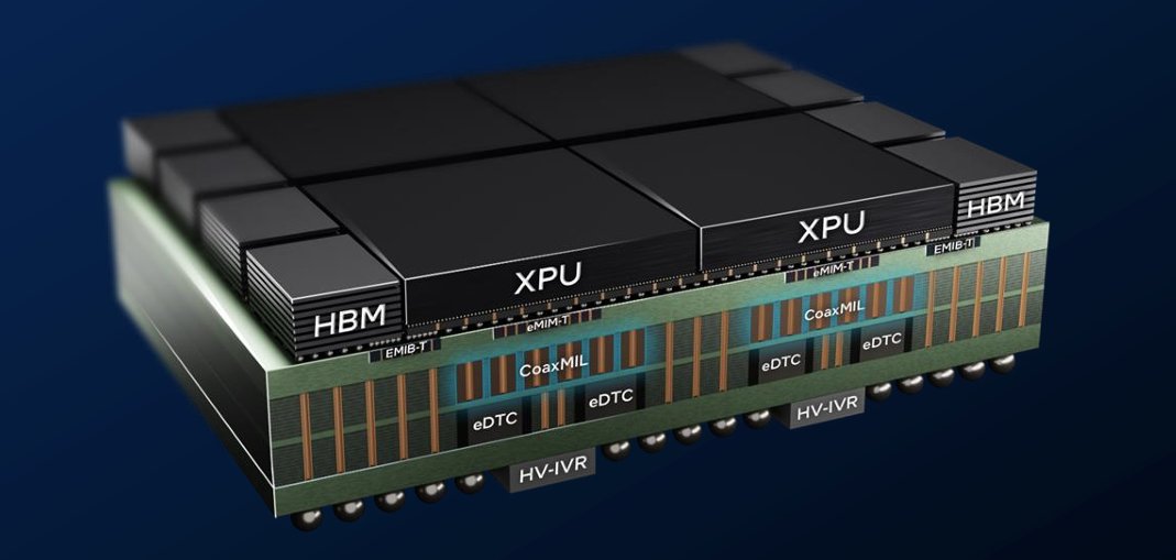
EMIB-T 供應鏈經濟學——英特爾正在打造下一個封裝生態系

這一步棋為何牽動全球 AI 供應鏈?

市場的反應很直接:消息傳出後台積電 ADR 單日漲逾 7%,法人也點名多家封測與載板廠受惠。背後的邏輯有三層:

1. 產能瓶頸:AI 晶片需求爆發,CoWoS 產能滿載,客戶排隊排到天邊。多一條「類 EMIB」技術路線,等於多一個出貨通道。

2. 專利與生態:英特爾的 EMIB 生態已吸引 Nvidia 評估採用,據報 Google 還向英特爾下了數百萬顆客製 AI 晶片的訂單。台積電若能用自有技術提供同等級方案,就能把客戶留在自己的生態圈。

3. 供應鏈擴散:先進封裝不再只是晶圓代工廠的遊戲——載板、封測、材料業者都成了戰略環節,ABF 載板甚至被形容為「戰略物資」。

投資與產業視角:如何分辨「真受惠」與「沾光題材」?

當一個技術趨勢發燒,股市總會出現大量「沾光股」。判斷真偽可以看三個問題:這家公司是否真的進入先進封裝供應鏈?訂單是確定的還是「可能」?技術門檻是否構成護城河?載板與封測廠的獲利能不能兌現,最終還是要看良率爬升與客戶驗證的實際進度,而不是新聞標題。

先進封裝的軍備競賽才剛開始。台積電挑戰英特爾、中國廠商強攻玻璃基板,全球供應鏈的勢力版圖正在重畫——誰能穩定量產、誰能綁住大客戶,誰就是下一輪 AI 晶片戰爭的贏家。

常見問題 (FAQ)

Q1:CoWoS 和 EMIB 到底差在哪?

CoWoS 用一整片矽中介層連接晶片與 HBM,面積大、成本高;EMIB 只在需要高速互連的位置嵌入小型矽橋,成本較低但技術複雜。兩者都是為了突破單一晶片面積極限而生的「多晶片」封裝方案。

Q2:為什麼摩爾定律放緩,先進封裝反而更重要?

電晶體微縮的成本與難度指數上升,廠商轉而靠「把多顆成熟製程的晶片封在一起」來提升整體效能。先進封裝等於在物理層面為晶片「疊 buff」,是延續效能成長的新路徑。

Q3:景碩是什麼公司?ABF 載板為何突然變重要?

景碩是 ABF 載板大廠。先進封裝與高階晶片都需要 ABF 載板作為「地基」,載板層數與精度直接決定封裝良率,因此從零組件一躍成為 AI 供應鏈的關鍵環節。

Q4:台積電做「類 EMIB」會影響 CoWoS 的地位嗎?

短中期不會——CoWoS 仍是 AI 加速器主流,需求遠大於供給。類 EMIB 更像是補足產能與成本彈性的第二條路線,讓台積電在不同客戶需求下提供更完整的選單。

Q5:一般投資人該怎麼看待這個趨勢?

先看訂單是否落實到財報,再判斷技術門檻。先進封裝是長線結構性趨勢,但供應鏈廠商良率爬升需要時間,短線漲幅往往領先基本面,追高前記得檢視估值。

留言

這個網誌中的熱門文章

Intel 14A Defect Density Is Its Best Since 22nm — Is Intel Back in the Leading-Edge Race?

One-sentence takeaway: Intel's 14A process is cutting defect density faster than any node since 22nm, and customers have moved from watching to asking about capacity — if risk production stays on track for H2 2027, it's the strongest signal yet that Intel is back in the leading-edge game. "We have not seen this performance since 22nm." When Intel CFO David Zinsner dropped that line at the Deutsche Bank 2026 technology conference, the semiconductor world took notice. 14A — Intel's first 1.4nm-class node — is backing up the company's comeback story with data, not slogans. What is 14A, and why it matters 14A is Intel's most advanced planned process node, a "1.4nm-class" technology targeting high-volume manufacturing in 2028. It packs three headline technologies: second-generation RibbonFET gate-all-around transistors, PowerDirect backside power delivery, and High-NA EUV lithography. In short, it's the most technically complex node Intel ...

Google's Antitrust Remedies Enter Deep Water: Breakup, AI Mode, and the Browser

Bottom line: The U.S. DOJ's remedies phase against Google is redefining the commercial rules of "search" — from Chrome's fate to AI distribution and the ad business, every step could reshape global tech. Google's search monopoly case has been called "the most important antitrust case of the internet era." In August 2024, a federal judge ruled Google violated antitrust law; now the remedies phase is in deep water. The DOJ's proposals include breaking up the ad business, divesting Chrome, and ending default search agreements — each step ripples through the entire tech industry. Timeline: from monopoly ruling to remedies In August 2024, the D.C. federal court ruled that Google violated the Sherman Act by paying billions annually to make Apple, Samsung, and others set Google as the default search engine. The remedies trial runs through 2026, with DOJ options including: Breaking up the ad business: Google's ad tech stack is accused of stifl...

Why Is NVIDIA Spending Billions to Buy Up America's "Dark Fiber"?

One-line conclusion: NVIDIA is reportedly spending $5–10 billion to acquire long-haul "dark fiber" networks across the United States, signaling that the AI infrastructure race is shifting from raw compute power to the networks that connect it. NVIDIA is reportedly acquiring long-haul "dark fiber" networks across the United States, with total capacity estimated at 7.6 Pbps and a price tag between $5 billion and $10 billion. The news sent optical communications stocks surging globally: Taiwan's optical module makers jumped on July 22, and three more hit the daily limit on July 23. Many now read this as the moment the AI arms race moved from "who has more GPUs" to "who owns the network." What Is Dark Fiber, and Why Buy Instead of Lease? Dark fiber refers to fiber-optic cable that has already been laid but has no transmission equipment installed and carries no optical signal . The fiber cores sit "dark" and dormant, waiting to...